Working Principles
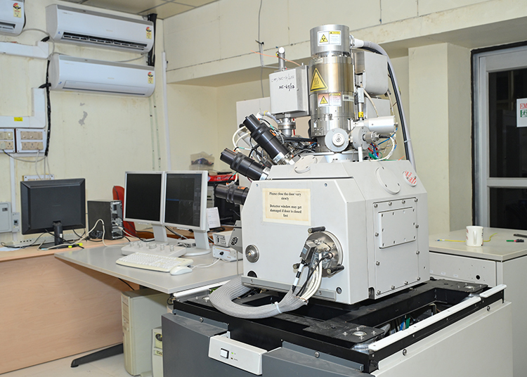
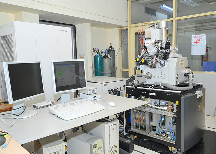
The FIB model D97NOVA 6000 combines the Scanning Electron Beam (SEM) and the Focused Ion Beam (FIB) in order to achieve analysis at nano-scale resolution. The instrument is equipped with different detectors, GIS systems and micromanipulator which make it ideal for to perform high-resolution imaging, nano-patterning, material deposition, milling, TEM lamella preparation etc.
Capabilities :
1. TEM lamella preparation
2. Site specific Cross sectional imaging , 3D Slice and View
3. Precision machining for micro tools
4. HR imaging, Low kV HR imaging , SEM/STEM imaging , Ion beam imaging
5. Nano-fabrication and Nano-patterning
FIB Charges (Excluding GST)
***This is an introductory price. The charges may be reviewed at yearly.
Operation |
IITK |
OUTSITE USER |
SEM ( 2 Hours) |
1500/- |
2000/- |
Milling (3 hours) |
2000/- |
3000/- |
** FIB Patterning requires a minimum 3 hours.
Information
- Faculty Incharge: Sudeep Bhattacharjee
- Lab Incharge: Mr. Jagtap P Bhimrao
Instrument Details
Make: ThermoFISHER Model: Model -D97NOVA 6000
Electron Beam Column Specification:
Electron Source :
Thermal Schottky Field-emitter.Accelerating
Voltage: Up to 30kV
Continuously variable Probe current:
Continuously variable in the range of :
0.8 pA – 100nA
Electron Beam Resolution:
10nm @ 30 kV (STEM Mode)
10 nm @ 1 kV
10 nm @ 15 kV
FIB Column Specification:
Accelerating Voltage:
Up to 30 kV,
continuously variableIon Gun:
Gallium liquid metal ion source
Available.Probe current:
It covers the range from 1 pA to 65 nA or larger.Imaging Resolution: 10 nm @ 30 kV
Book Facilities
Please Download Facility forms
- Booking form : Job Form (http://172.28.37.81/booking/)
- Charge & Instruction : PDF (http://172.28.37.81/booking/doc/17.pdf)