Texture Lab
Location: ACMS 112
Texture Lab consists of two equipment
# Four Circle diffractometer (see links on right side for booking slots)
# FE-SEM with Orientation Imaging Microscopy (see links on right side for booking slots)
The Texture Facility at ACMS aims to provide bulk texture measurement using X-ray diffraction and micro-texture measurement using Scanning Electron Microscopy based Electron Back Scatter Diffraction setup. The facility provides end to end solution for texture and stress determination at multiple length scales as well as detailed analysis to draw concrete conclusions. The micro-texture facility on a Field Emission Gun Scanning Electron Microscope (FE-SEM) with spot size of 20 nm allows High Resolution Electron Back Scatter Diffraction (HR-EBSD) for better characterization of sub-microcrystalline and nano materials. The ability to carry out microstructure and micro-texture measurement as a function of deformation and temperature by means of an in-situ GATAN device enables combinatorial studies involving microstructure, texture and chemistry (by energy dispersive spectroscopy in SEM) in deformation, recrystallization and phase transformation of variety of materials.
The facility is equipped with a Rigaku Four circle diffractometer Ultima capable of determining pole figures for bulk as well as thin film samples. In addition, the diffractometer can carry out residual stress measurement on bulk and thin film samples. Detailed analysis of thin films using rocking curves and combinatorial analysis of stress and orientation along with quality of epitaxial thin films can be obtained using reciprocal space map. In addition, different sources like copper and cobalt are available which ensure that different class of materials from iron and steel, titanium and its alloys with Cobalt source and other non-ferrous materials like aluminium, copper and their alloys can be studied without fluorescence using a Copper source. The diffractometer is equipped with state of the art optics to enable above mentioned modes of measurement that cover almost all the texture and stress measurement needs of bulk and thin film samples.
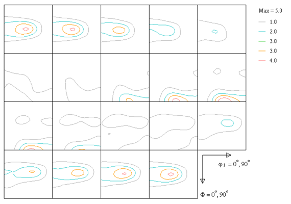 |
φ2 sections of Orientation Distribution Function for a 80% rolled austenitic stainless steel sample with cubic crystal symmetry and orthotropic sample symmetry. The ODF was determined using incomplete 111, 200, 220 and 113 pole figures till inclination of 70 degree. |
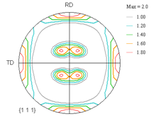 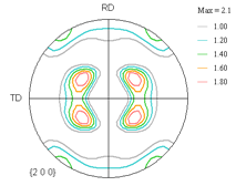 |
Complete Pole figures determined from Orientation distribution Function with cubic-orthotropic crystal and sample symmetry respectively of 316 austenitic stainless steel sample. |
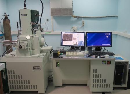
The high resolution secondary as well as backscattered electron images shall now be possible with the new addition of the FE-SEM. The FE-SEM is equipped with SE, BSE and EDS detector in addition to EBSD, tensile stage module and a heating stage. With EBSD based Orientation Imaging Microscopy (OIM), the equipment has an unmatched capability of micro-texture analysis. The tensile stage makes it possible to carry out in-situ tensile testing and the heating stage can be used to take the images at up to 500 degree Celsius.
FE-SEM
Electron Backscattered Diffraction based Orientation Imaging Microscopy
Microstructural characterization is central to any kind of experimental research in Materials Science. Electron Microscope and particularly scanning electron microscope (SEM) is the backbone for most of these characterizations. SEM is used not only for generating secondary electron images of the surface of the sample at very high magnifications; it is also used for investigating topographical and compositional contrast in materials using back-scattered electrons. Apart from above mentioned qualitative studies, SEMs can now also be used for quantitative analysis, with the aid of attachments like Energy Dispersive Spectroscopy (EDS)/ Electron Back Scattered Diffraction (EBSD)/ Wavelength Diffraction Spectroscopy (WDS).
In order to fully exploit the prowess of microscopy, our FE-SEM is also equipped with attachments like EDS and EBSD. Apart from this, an in-situ tensile stage is available to conduct tensile test and heating and collect EBSD images simultaneously.
| OIM of annealed sample of Copper and the inset shows the color index of various orientations Orientation map overlayed on band contrast image for copper sample passed through one cycle of Constrained Grooved Pressing (CGP) |
EBSD based Orientation Imaging Microscopy can provide several detailed information regarding microstructure which cannot be obtained by simple microscopy. It allows one to find the grain size, misorientation, micro-texture, characterize grain boundaries. These information can, in turn, be utilized to understand the effect of processing on microstructure at lattice level and also help understand microstructural evolution.
In the figure shown above, top image is an OIM for annealed copper. Here each color represents a unique orientation which can be identified from the inverse pole figure shown in inset. This map contains in itself detailed information on not only the orientation along the perpendicular direction, but also the azimuthal orientation of each and every point. A contiguous region of similar orientation, thus depicts a grain, and the difference in orientation between these grains gives misorientation. Moreover, for the misorientation all the five parameters can be obtained and not just the axis-angle pair of misorientation.
Various Analysis that can be carried out using EBSD based OIM are:
a) Understanding variation of Coincident Site Lattice boundaries across sample space and processing conditions
b) Understanding variation of grain size and hence effect of deformation across sample space and processing conditions
c) Band contrast shows the quality of signal obtained which is directly proportional to the deformation state of the sample. Hence one can understand the state of stress inside the sample by studying band contrast.
d) Another parameter used for studying deformation state of the sample is “Average misoreintation”. A highly deformed grain will have continuous deviation in orientation from point to point. The average of these can be calculated to obtain not only the overall deformation state (or recrystallized state), but also to ascertain regions of high and low strains.
e) Since, EBSD can give us orientation of each and every point, one can also find orientation correlation between two phases or matrix and precipitate.
Instrument: Four Circle Diffractometer
Model/Supplier:Rigaku
a) Texture and Residual Stress measurementb) X-ray reflectivity
c) Rocking Curve
d) Reciprocal Space Mapping
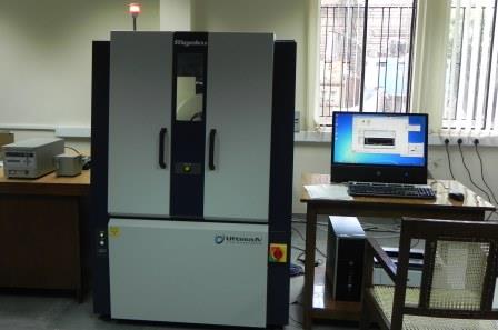  |
Rigaku Ultima for texture and residual stress measurement (with micro-focus source, X-ray reflectivity, Rocking Curve and Reciprocal Space Mapping for epitaxial thin films) |
Rigaku table top diffractometer will be the workhorse diffractometer for the facility and will be used for training and research purpose. All users of the facility will be exposed to the basic principles of X-ray diffraction and it's practical applications using this equipment. The users will also learn the nuances of data collection and data analysis on this equipment. Once the basics of X-ray diffraction are covered, they will graduate to a specific technique on either or both the advanced diffractometers to carry out specialized tests like thin film diffraction, high temperature diffraction, small angle scattering, texture, residual stress, rocking curve and reciprocal space mapping on a case to case basis. The facility aims to produce a steady stream of trained individuals who can shoulder the operation of X-ray equipments and carry out cutting edge research at the facility as well as in their departments at IIT Kanpur. The centre aims to promote DIY concept for handling sophisticated research equipments by research scholars to aid the yield as well as quality of research carried out on campus.
CONTACT
| Convener: Prof. N P Gurao([email protected]) | Internal: 6688 |
| Staff: Ashish Kumar Tiwari([email protected]) | Internal: 7814 |
| Staff: Mitesh Shrotriy([email protected]) | Internal: 7814 |
Instrument: Field Emission FE-SEM with in situ Tensile Testing and EBSD
Model/Supplier: JSM-7100F; JEOL
  |
This facility is used in two modes: |
Features
#SE Resolution: 3nm at 15kV/5nA
#Magnification: 10x to 1000000x
#Accelerating Voltage: 0.5 to 30kV
#Elemental mapping by EDS
#Micro-texture analysis by EBSD with smallest step size of 10 nm possible
#Combinatorial EBSD and EDS
#GATAN Tensile stage of 5kN capacity and temperature of 500 degree Celsius
How to book slots
FESEM(EBSD) and Rigaku four circle slots can only be booked online in three steps.
Click the link "Request Slots" and fill in the details as requested. You can select an empty slot upto 1 month in advance and only for week days. You can check the availability of slots using the module "Check Slot" or you can check "Booking status" to see all the slots which have already been taken.
Once you submit the request, an invoice will be generated. Please submit this invoice to Mr. M. Siva kumar (Ph. 6031) for Fesem(EBSD) and Mr D.D Pal (Ph. 7814)For Rigaku four within 48 hours. If you do not submit within this time lime, your slot will get automatically cancelled and will be open for booking again.
Lab-in-charge will then accept your booking and you can check your status at "Booking status".
Please note that we will soon make this procedure paperless, but until then you will have to submit the paper invoice.
Following slots are available to users:
| Slots for FE-SEM 9.30 to 11.30 11.30 to 1.30 2.30 to 4.30 | slotsforRigakuFourCircle 9.30 to 12.30 2.00 to 5.00 |
|---|
Non-IITK Users:
1. The online booking is valid only for IITK users.
2. Non-IITK users need to send an email to Mr. Sivakumar ([email protected]) and D.D Pal([email protected]) with details of the sample. Users are responsible for proper preparation of their sample. Once we are satisfied that your sample is ready and suitable for our EM, we will book a slot for you and convey you the date and time and the charges for the slot. Please see "User Charges" to get an estimate of the charges for utilizing the facility.
3. Non-IITK Users must send in advance, a Demand Draft, in favor of "Registrar, IIT Kanpur" for the requisite user charges (inclusive of service taxes, 12.36%)
4. If you have an urgency and you want to get your samples characterized on a speedy basis, then you may be allowed to come along with your prepared sample and the demand draft. However your must confirm with Mr Sivakumar ([email protected]) before coming here to the facility.
CONTACT
| Convener: Prof. S. Shekhar ([email protected]) | Internal:6528 |
| Lab Incharge: M. Siva Kumar ([email protected]) | Internal:6284,6031 |
| Mitesh Shrotriy([email protected]) | Internal:6284,6293 |
| Jaikishan([email protected]) | Internal:6284,6293 |

